产品详情
- RF 频率范围: 0.6GHz to 2.7GHz
- 获得 at 2.5GHz:
- 29.5dB typical max 获得 in non-bypass mode
- 10.9dB typical max 获得 in bypass mode
- DSA Control:
- DSA0: Single 6dB 步 via SPI/I3C control
- DSA1: Single 6dB 步 via 1-bit external pin control
- DSA2: 29dB 范围 in 1dB 步s via SPI/I3C control
- DSA3: 18dB 范围 in 6dB 步s via 2-bit external pin control
- +39dBm OIP3 at 2.5GHz
- NF at 2.5GHz
- 3.2dB typical in non-bypass mode
- 8.9dB typical in bypass mode
- +19.7dBm OP1dB at 2.5GHz
- ICC = 372mA
- Standby Mode for power savings with 9mA standby current
- 50Ω single-ended input/输出阻抗s
- 1.8V logic 支持
- Operating temperature 范围: -40 °C to +105 °C
- 7mm × 7mm 48-LGA 包裹
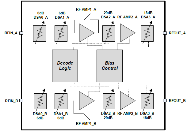
The F0443 is a 高ly integrated 0.6GHz to 2.7GHz dual-channel RF digital variable 获得 amplifier designed for use in diversity/MIMO receivers. The F0443 provides two independent receiver paths each with 29.5dB typical maximum 获得 and 3.2dB NF at 2.5GHz.
For each path, 获得 control is split into four separate digital 步 attenuators: DSA0 provides 6dB of attenuation in a single 步 using SPI/I3C control. Its counterpart, DSA1, also provides 6dB of attenuation in a single 步 but it is programmed instead using an external direct control pin. DSA2 yields 29dB of SPI/I3C-controlled attenuation in 1dB 步s, while its counterpart, DSA3, includes 18dB attenuation in 6dB 步s programmed via two external control pins. The device offers +39dBm nominal 输出IP3 at 2.5GHz using 372mA total ICC for two active paths with a +5V 电源电压.
The F0443 is 包裹d in a 7mm × 7mm, 48-LGA with 50Ω single-ended RF input and RF 输出阻抗s for easy integration into the signal path.
.jpg)
您还有其他问题吗?
我们在这里帮助您探索可能性,优化性能并推动技术进步。今天伸出援手!
与销售人员交谈