产品详情
- Independent dual-path operation
- RF output frequency: 450MHz to 2800MHz
- 18.3dB typical maximum 获得 (no attenuation)
- +31dBm OIP3 (no attenuation)
- +14dBm Output P1dB (no attenuation)
- 13dB NF corresponds to -142.5dBm/Hz output noise floor (no attenuation)
- Output noise floor -152.3dBm/Hz (VVA = 14dB, DSA = 1dB)
- Channel Isolation: 47dB
- DSA with 31dB total 获得 范围 in 1dB 步s
- Multiple VVAs with 32dB 获得 范围 controlled by on-chip SPI controlled 11-bit DAC
- Variable 获得 amplifier (VGA) is comprised of DSAs, VVAs, and a fixed-获得 amplifier
- I lead Q by 90 degrees for 高 side LO injection
- 支持s ZIF or CIF 建筑学s
- Common-mode voltage 范围: +0.1V to +0.8V
- Integer-N and Fr行动al-N Synthesizer
- Direct 110? differential driven from I/Q DAC
- 50? single-ended RF 输出阻抗
- Internal or external LO 选择
- +3.3V 电源电压 at 685mA (LO_Out not turned on)
- Specified case temperature: -20°C to +115°C
- 10 × 10 mm, 68-VFQFPN 包裹
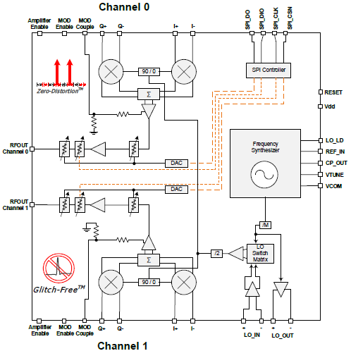
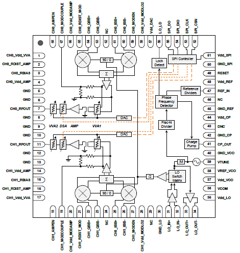
The F159V is a Dual-Path Integrated TRx IC that has an operating 频率范围 of 450MHz to 2800MHz. The device provides two independent transmit paths each with 18.3dB typical maximum 获得 with corresponding output noise floor of -142.5dBm/Hz, +31dBm OIP3, and +14dBm output P1dB designed to operate with a single +3.3V supply while consuming only 685mA DC current. Each signal path includes a quadrature modulator, voltage variable attenuator (VVA), digital 步 attenuator (DSA), and a fixed 获得 amplifier. The device 支持s a total of 32dB VVA adjustment 范围 using a SPI-controlled 11-bit DAC, and each DSA has 31dB 获得 control 范围 in 1dB 步s using SPI control.
An on-chip frequency synthesizer is 分享d by both paths and is optimized for use in multi-carrier, multi-mode FDD and TDD base station transmitters achieving GSM-grade performance. The synthesizer offers both an integer mode and fr行动al mode. It requires an external loop filter and an external reference oscillator in the 频率范围 of 10MHz to 250MHz.
The F159V is 包裹d in a 10mm x 10mm, 68-pin QFN with 110? differential drive from external I/Q DACs and single-ended 50? RF 输出阻抗 for ease of integration into the signal-path lineup for each of the two transmitter paths. Each path has independent power supply control thereby allowing optimum power efficiency.
产品文档
类型
姓名
日期
动作
2025-08-25
F159V 数据表
2025-08-25
PCN# : A1709-03 Add Alternate Assembly 地点 on F159V
2025-08-25
PLC# : 240021 End-of-Life (EOL) process on 选择 部件号s
Boards and Kits
.PNG)
Evaluation Board for the F159V Integrated TRx IC
The F159VEVB is a fully populated test board enabling easy evaluation of the F159V Integrated TRx IC.
您还有其他问题吗?
我们致力于帮助您探索各种可能性,优化性能,并推动技术进步。立即联系我们!
与销售人员交谈