产品详情
- RF 频率范围: 3.3GHz to 4.2GHz
- Dual path RF amp and DSAs for diversity/MIMO receivers
- < 2dB overshoot between DSA transitions
- 13dB typical max 获得 at 3.6GHz
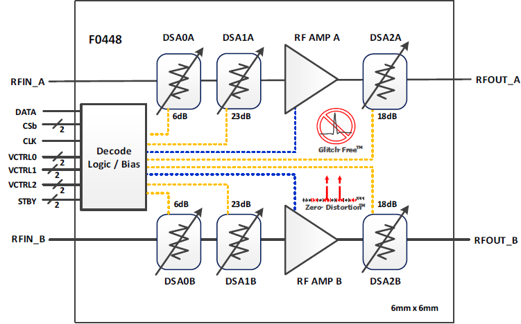
- DSA0: Single 6dB coarse 步
- DSA1: 23dB total 获得 范围 in 1dB 步s
- DSA2: 18dB 获得 范围 in 6dB 步s
- +37dBm OIP3 at 3.6GHz
- 6dB noise figure at 3.6GHz
- +5V 电源电压
- ICC = 220mA
- Independent standby: 7mA standby current
- SPI interface for DSA1
- 1-bit control for DSA0
- 2-bit control for DSA2
- 50? input and 输出阻抗
- Broadband, internally matched
- Temperature 范围: -40 °C to +105 °C
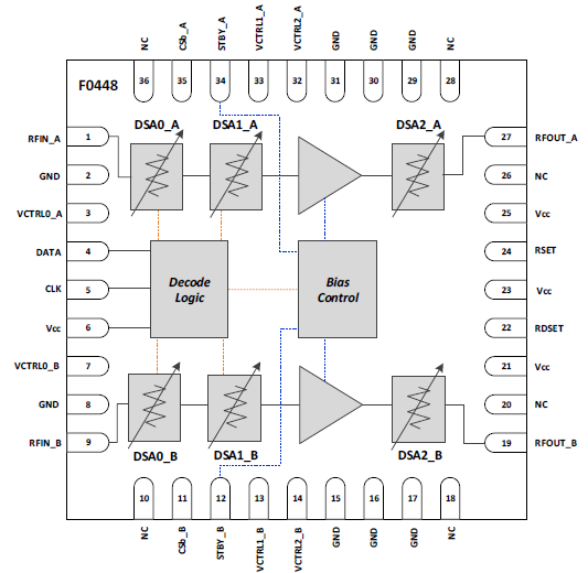
- 6mm x 6mm, 36-QFN 包裹
The F0448 is a 3.3GHz to 4.2GHz dual RF digital variable 获得 amplifier (DVGA) designed for use in receivers. This dual RF DVGA provides two independent receiver paths each with 13dB typical maximum 获得 and 6dB noise figure designed to operate with a single +5V supply. For each path, 获得 control is split into 3 separate attenuators; DSA0 a single 6dB 步 using a single control pin, DSA1 a 23dB SPI-controlled 获得 adjustment in 1dB 步s, and DSA2 includes 18dB attenuation in 6dB 步s controlled using two control pins. F0448 offers +37dBm nominal 输出IP3 using 220mA total ICC. This device is 包裹d in a 6mm x 6mm, 36-QFN with 50? single-ended RF input and RF 输出阻抗s for ease of integration.
- Multi-mode, Multi-carrier Receivers
- PHS/PAS Base Stations
- Distributed Antenna Systems
- Digital Radio
产品文档
类型
姓名
日期
动作
2025-08-25
AN-874 Using the TRL Calibration Board for the F0480 Matched Broadband RF VGA
2025-08-25
RF 产品 Evaluation System (EVS) Digital Control Software
2025-08-25
AN-1013 F0448 GUI Automation
2025-08-25
PCN# : 210023 Add Alternate Assembly 地点s on 选择 VFQFN 包裹s
Boards and Kits
.png)
Evaluation Board for F0448 Dual Matched Broadband RF DVGA
The F0448EVB is a fully populated evaluation board which allows the customer to easily evaluate the F0448 Dual Matched Broadband RF DVGA. The attenuation setting may be set using the F0448's serial control input. Header pins on the evaluation board allow setting standby mode without off-board connections to the control inputs.
The F0448EVS is a complete hardware and software solution that allows customers to digitally control the F0448EVB with the USB output on a computer. The kit includes the F0448EVB board, as well as a USB Digital Control Board and interface cables.
您还有其他问题吗?
我们致力于帮助您探索各种可能性,优化性能,并推动技术进步。立即联系我们!
与销售人员交谈